
8085 Microprocessor
- The Tech Platform

- Oct 7, 2020
- 7 min read
The Intel 8085 ("eighty-eighty-five") is an 8-bit microprocessor produced by Intel and introduced in March 1976. It is a software-binary compatible with the more-famous Intel 8080 with only two minor instructions added to support its added interrupt and serial input/output features.
It has the following configuration −
8-bit data bus
16-bit address bus, which can address upto 64KB
A 16-bit program counter
A 16-bit stack pointer
Six 8-bit registers arranged in pairs: BC, DE, HL
Requires +5V supply to operate at 3.2 MHZ single phase clock
It is used in washing machines, microwave ovens, mobile phones, etc.
8085 Microprocessor – Functional Units
8085 consists of the following functional units −
Accumulator
It is an 8-bit register used to perform arithmetic, logical, I/O & LOAD/STORE operations. It is connected to internal data bus & ALU.
Arithmetic and logic unit
As the name suggests, it performs arithmetic and logical operations like Addition, Subtraction, AND, OR, etc. on 8-bit data.
General purpose register
There are 6 general purpose registers in 8085 processor, i.e. B, C, D, E, H & L. Each register can hold 8-bit data.
These registers can work in pair to hold 16-bit data and their pairing combination is like B-C, D-E & H-L.
Program counter
It is a 16-bit register used to store the memory address location of the next instruction to be executed. Microprocessor increments the program whenever an instruction is being executed, so that the program counter points to the memory address of the next instruction that is going to be executed.
Stack pointer
It is also a 16-bit register works like stack, which is always incremented/decremented by 2 during push & pop operations.
Temporary register
It is an 8-bit register, which holds the temporary data of arithmetic and logical operations.
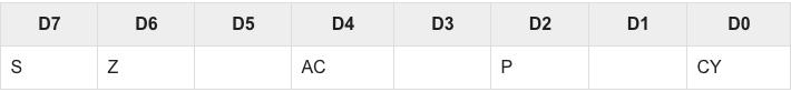
Flag register
It is an 8-bit register having five 1-bit flip-flops, which holds either 0 or 1 depending upon the result stored in the accumulator.
These are the set of 5 flip-flops −
Sign (S)
Zero (Z)
Auxiliary Carry (AC)
Parity (P)
Carry (C)
Its bit position is shown in the following table −
Instruction register and decoder
It is an 8-bit register. When an instruction is fetched from memory then it is stored in the Instruction register. Instruction decoder decodes the information present in the Instruction register.
Timing and control unit
It provides timing and control signal to the microprocessor to perform operations. Following are the timing and control signals, which control external and internal circuits −
Control Signals: READY, RD’, WR’, ALE
Status Signals: S0, S1, IO/M’
DMA Signals: HOLD, HLDA
RESET Signals: RESET IN, RESET OUT
Interrupt control
As the name suggests it controls the interrupts during a process. When a microprocessor is executing a main program and whenever an interrupt occurs, the microprocessor shifts the control from the main program to process the incoming request. After the request is completed, the control goes back to the main program.
There are 5 interrupt signals in 8085 microprocessor: INTR, RST 7.5, RST 6.5, RST 5.5, TRAP.
Serial Input/output control
It controls the serial data communication by using these two instructions: SID (Serial input data) and SOD (Serial output data).
Address buffer and address-data buffer
The content stored in the stack pointer and program counter is loaded into the address buffer and address-data buffer to communicate with the CPU. The memory and I/O chips are connected to these buses; the CPU can exchange the desired data with the memory and I/O chips.
Address bus and data bus
Data bus carries the data to be stored. It is bidirectional, whereas address bus carries the location to where it should be stored and it is unidirectional. It is used to transfer the data & Address I/O devices.
8085 Architecture
We have tried to depict the architecture of 8085 with this following image −


The following image depicts the pin diagram of 8085 Microprocessor −


The pins of a 8085 microprocessor can be classified into seven groups −
Address bus
A15-A8, it carries the most significant 8-bits of memory/IO address.
Data bus
AD7-AD0, it carries the least significant 8-bit address and data bus.
Control and status signals
These signals are used to identify the nature of operation. There are 3 control signal and 3 status signals.
Three control signals are RD, WR & ALE.
RD − This signal indicates that the selected IO or memory device is to be read and is ready for accepting data available on the data bus.
WR − This signal indicates that the data on the data bus is to be written into a selected memory or IO location.
ALE − It is a positive going pulse generated when a new operation is started by the microprocessor. When the pulse goes high, it indicates address. When the pulse goes down it indicates data.
Three status signals are IO/M, S0 & S1.
IO/M
This signal is used to differentiate between IO and Memory operations, i.e. when it is high indicates IO operation and when it is low then it indicates memory operation.
S1 & S0
These signals are used to identify the type of current operation.
Power supply
There are 2 power supply signals − VCC & VSS. VCC indicates +5v power supply and VSS indicates ground signal.
Clock signals
There are 3 clock signals, i.e. X1, X2, CLK OUT.
X1, X2 − A crystal (RC, LC N/W) is connected at these two pins and is used to set frequency of the internal clock generator. This frequency is internally divided by 2.
CLK OUT − This signal is used as the system clock for devices connected with the microprocessor.
Interrupts & externally initiated signals
Interrupts are the signals generated by external devices to request the microprocessor to perform a task. There are 5 interrupt signals, i.e. TRAP, RST 7.5, RST 6.5, RST 5.5, and INTR. We will discuss interrupts in detail in interrupts section.
INTA − It is an interrupt acknowledgment signal.
RESET IN − This signal is used to reset the microprocessor by setting the program counter to zero.
RESET OUT − This signal is used to reset all the connected devices when the microprocessor is reset.
READY − This signal indicates that the device is ready to send or receive data. If READY is low, then the CPU has to wait for READY to go high.
HOLD − This signal indicates that another master is requesting the use of the address and data buses.
HLDA (HOLD Acknowledge) − It indicates that the CPU has received the HOLD request and it will relinquish the bus in the next clock cycle. HLDA is set to low after the HOLD signal is removed.
Serial I/O signals
There are 2 serial signals, i.e. SID and SOD and these signals are used for serial communication.
SOD (Serial output data line) − The output SOD is set/reset as specified by the SIM instruction.
SID (Serial input data line) − The data on this line is loaded into accumulator whenever a RIM instruction is executed.
Addressing Modes in 8085
These are the instructions used to transfer the data from one register to another register, from the memory to the register, and from the register to the memory without any alteration in the content.
Addressing modes in 8085 is classified into 5 groups −
Immediate addressing mode
In this mode, the 8/16-bit data is specified in the instruction itself as one of its operand. For example: MVI K, 20F: means 20F is copied into register K.
Register addressing mode
In this mode, the data is copied from one register to another. For example: MOV K, B: means data in register B is copied to register K.
Direct addressing mode
In this mode, the data is directly copied from the given address to the register. For example: LDB 5000K: means the data at address 5000K is copied to register B.
Indirect addressing mode
In this mode, the data is transferred from one register to another by using the address pointed by the register. For example: MOV K, B: means data is transferred from the memory address pointed by the register to the register K.
Implied addressing mode
This mode doesn’t require any operand; the data is specified by the opcode itself. For example: CMP.
Interrupts in 8085
Interrupts are the signals generated by the external devices to request the microprocessor to perform a task. There are 5 interrupt signals, i.e. TRAP, RST 7.5, RST 6.5, RST 5.5, and INTR.
Interrupt are classified into following groups based on their parameter −
Vector interrupt − In this type of interrupt, the interrupt address is known to the processor. For example: RST7.5, RST6.5, RST5.5, TRAP.
Non-Vector interrupt − In this type of interrupt, the interrupt address is not known to the processor so, the interrupt address needs to be sent externally by the device to perform interrupts. For example: INTR.
Maskable interrupt − In this type of interrupt, we can disable the interrupt by writing some instructions into the program. For example: RST7.5, RST6.5, RST5.5.
Non-Maskable interrupt − In this type of interrupt, we cannot disable the interrupt by writing some instructions into the program. For example: TRAP.
Software interrupt − In this type of interrupt, the programmer has to add the instructions into the program to execute the interrupt. There are 8 software interrupts in 8085, i.e. RST0, RST1, RST2, RST3, RST4, RST5, RST6, and RST7.
Hardware interrupt − There are 5 interrupt pins in 8085 used as hardware interrupts, i.e. TRAP, RST7.5, RST6.5, RST5.5, INTA.
Note − NTA is not an interrupt, it is used by the microprocessor for sending acknowledgement. TRAP has the highest priority, then RST7.5 and so on.
Interrupt Service Routine (ISR)
A small program or a routine that when executed, services the corresponding interrupting source is called an ISR.
TRAP
It is a non-maskable interrupt, having the highest priority among all interrupts. By default, it is enabled until it gets acknowledged. In case of failure, it executes as ISR and sends the data to backup memory. This interrupt transfers the control to the location 0024H.
RST7.5
It is a maskable interrupt, having the second highest priority among all interrupts. When this interrupt is executed, the processor saves the content of the PC register into the stack and branches to 003CH address.
RST 6.5
It is a maskable interrupt, having the third highest priority among all interrupts. When this interrupt is executed, the processor saves the content of the PC register into the stack and branches to 0034H address.
RST 5.5
It is a maskable interrupt. When this interrupt is executed, the processor saves the content of the PC register into the stack and branches to 002CH address.
INTR
It is a maskable interrupt, having the lowest priority among all interrupts. It can be disabled by resetting the microprocessor.
When INTR signal goes high, the following events can occur −
The microprocessor checks the status of INTR signal during the execution of each instruction.
When the INTR signal is high, then the microprocessor completes its current instruction and sends active low interrupt acknowledge signal.
When instructions are received, then the microprocessor saves the address of the next instruction on stack and executes the received instruction.
THE TECH PLATFORM


Comments